
12-Layer High-Speed PCB Built on Megtron6 (M6) Laminate with both sided 35μm copper weight using in millimeter-wave radar
Product Description: 12-Layer High-Speed PCB Built on Megtron6 (M6) Laminate
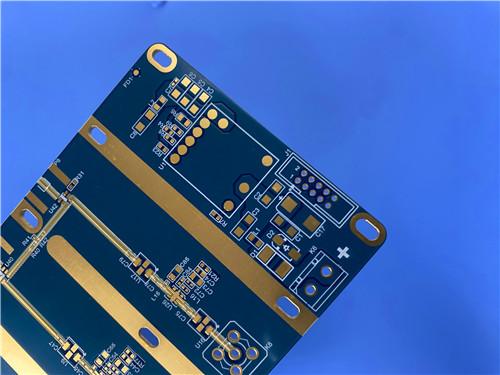
This 12-layer PCB, built using Megtron6 (M6) high-speed, low-loss laminate, offers a cutting-edge solution for applications requiring exceptional signal integrity, thermal reliability, and high-frequency performance. Its robust construction, precise impedance control, and compliance with IPC-Class-3 standards make it an ideal choice for 5G communication systems, automotive electronics, data centers, and aerospace applications. Below, we analyze its features, advantages, and disadvantages.
Key Construction Details
| Parameter | Specification |
| Layer Count | 12 layers |
| Base Material | Megtron6 (M6) |
| Dimensions | 220mm x 60mm (±0.15mm) |
| Finished Thickness | 2.12mm |
| Copper Weight | Outer: 1oz (35μm), Inner: 0.5oz/1oz |
| Minimum Trace/Space | 3/3 mils |
| Minimum Hole Size | 0.2mm |
| Via Plating Thickness | 25μm |
| Vias | 0.2mm/0.4mm filled with resin and capped plating |
| Surface Finish | ENIG (Electroless Nickel Immersion Gold) |
| Solder Mask | Top: Blue, Bottom: Blue |
| Silkscreen | Top: White, Bottom: White |
| Electrical Testing | 100% tested before shipment |
PCB Stackup
| Layer | Material | Thickness |
| Copper Layer 1 | Copper (1oz) | 35μm |
| Prepreg Layer 1 | R-5670 1080 (68%) | 81.4μm |
| Copper Layer 2 | Copper (1oz) | 35μm |
| Core Layer 1 | M6 R5775G (HVLP) | 75μm |
| Copper Layers 3-10 | Copper (0.5oz) | 17μm |
| Core Layers | M6 R5775G (HVLP) | 75-400μm |
| Copper Layer 11 | Copper (1oz) | 35μm |
| Prepreg Layer 2 | R-5670 1080 (68%) | 81.4μm |
| Copper Layer 12 | Copper (1oz) | 35μm |
Advantages
High-Speed and Low-Loss Performance
- Megtron6 laminate provides a low dielectric constant (Dk) of 3.34 at 13GHz and a low dissipation factor (Df) of 0.0037 at 13GHz. This ensures minimal signal loss and high-speed signal integrity for 5G, radar, and server applications.
- The material’s high Tg (>185°C) and thermal decomposition temperature (Td) of 410°C allow it to perform reliably in high-temperature environments.
Flexible Design Compatibility
- The use of Megtron6, which is compatible with traditional FR-4 processing techniques, reduces manufacturing complexity and cost compared to other high-speed materials.
- The PCB supports multi-layer designs ranging from 4 to 30 layers, making it suitable for various complex applications.
Wide Application Range
- 5G base stations (millimeter-wave antennas, RF front ends).
- Automotive electronics (77GHz radar, ADAS).
- Data centers (high-speed servers, optical modules).
- Aerospace (satellite communication, high-frequency radar systems).
- Consumer electronics (Wi-Fi 6E/7 routers, AR/VR devices).
Disadvantages
The use of Megtron6 laminates and high-precision construction increases production costs, making this PCB less suitable for cost-sensitive applications.
The 3/3 mil trace/space, resin-filled vias, and 12-layer stackup demand advanced manufacturing processes, limiting availability to specialized manufacturers.
The PCB is optimized for high-speed and high-reliability environments, making it over-engineered for simpler or low-frequency designs.
Conclusion
The 12-layer Megtron6 PCB is a high-performance, high-frequency solution tailored for demanding industries like 5G, automotive, aerospace, and HPC. Its low dielectric loss, precise impedance control, and thermal reliability ensure top-tier performance in critical applications. While it offers exceptional capabilities, the higher cost and complex manufacturing requirements may limit its use in general-purpose or low-budget designs.
Get in Touch
Have questions about our products or want to discuss a custom order? Our team is ready to help you.