
SP-Face 11-12 Un-Doped N-Type Free-Standing GaN Single Crystal Substrate Resistivity 0.05 Ω·cm Macro Defect Density 0cm⁻²
5*10mm2 SP-face (11-12) Un-doped n-type free-standing GaN single crystal substrate Resistivity < 0.05 Ω·cm Power device/laser wafer
Overview
Because GaN transistors are able to turn on faster than silicon transistors, they are able to reduce the losses caused by this transition. Another way that GaN reduces switching loss is through the absence of a body diode.
GaN is growing in importance because of its ability to offer significantly improved performance across a wide range of applications while reducing the energy and the physical space needed to deliver that performance when compared with conventional silicon technologies.
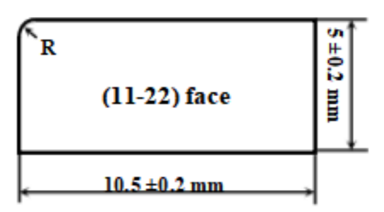
| (11-22) face Free-standing GaN Substrates | ||||
| Item |
GaN-FS-SP-U-S
|
GaN-FS-SP-N-S
|
GaN-FS-SP-SI-S |
Remarks: A circular arc angle (R < 2 mm) is used for distinguishing the front and back surface. |
| Dimensions | 5 x 10 mm2 | |||
| Thickness | 350 ±25 µm | |||
| Orientation |
(11-22) plane off angle toward M-axis 0 ±0.5° (11-22) plane off angle toward C-axis - 1 ±0.2° |
|||
| Conduction Type | N-type | N-type | Semi-Insulating | |
| Resistivity (300K) | < 0.1 Ω·cm | < 0.05 Ω·cm | > 106 Ω·cm | |
| TTV | ≤ 10 µm | |||
| BOW | - 10 µm ≤ BOW ≤ 10 µm | |||
| Front Surface Roughness |
< 0.2 nm (polished); or < 0.3 nm (polished and surface treatment for epitaxy) |
|||
| Back Surface Roughness |
0.5 ~1.5 μm option: 1~3 nm (fine ground); < 0.2 nm (polished) |
|||
| Dislocation Density | From 1 x 10⁵ to 3 x 106 cm-2 | |||
| Macro Defect Density | 0 cm-2 | |||
| Useable Area | > 90% (edge exclusion) | |||
| Package | Packaged in a class 100 clean room environment, in 6 PCS container, under a nitrogen atmosphere | |||
Appendix: The diagram of miscut angle

If δ1= 0 ±0.5°, then (11-22) plane off angle toward M-Axis is 0 ±0.5°.
If δ2= - 1 ±0.2°, then (11-22) plane off angle toward C-Axis is - 1 ±0.2°.
About Us
We specialize in processing a variety of materials into wafers, substrates and customized optical glass parts.components widely used in electronics, optics, opto electronics and many other fields. We also have been working closely with many domestic and oversea universities, research institutions and companies, provide customized products and services for their R&D projects. It's our vision to maintaining a good relationship of cooperation with our all customers by our good reputations.
FAQ
Q: Are you trading company or manufacturer ?
We are factory.
Q: How long is your delivery time?
Generally it is 3-5 days if the goods are in stock.
or it is 7-10 days if the goods are not in stock, it is according to quantity.
Q: Do you provide samples ? is it free or extra ?
Yes, we could offer the sample for free charge but do not pay the cost of freight.
Q: What is your terms of payment ?
Payment <=5000USD, 100% in advance.
Paymen >=5000USD, 80% T/T in advance , balance before shippment.
Get in Touch
Have questions about our products or want to discuss a custom order? Our team is ready to help you.