
Photonic Crystal Atomic Layer Deposition Equipment In Optics Industry
Atomic Layer Deposition in Optics Industry
Applications
| Applications | Specific Purpose |
| Optics | Optical components |
| Photonic crystal | |
| Electroluminescent display | |
| Surface-enhanced Raman spectroscopy | |
| Transparent conductive oxide | |
Luminous layer, passivation layer, filter protection layer, anti-reflective coating, anti-UV |
Working Principle
Atomic layer deposition (ALD), originally called atomic layer epitaxy, also called atomic layer chemical vapor
deposition (ALCVD), is a special form of chemical vapor deposition (CVD). This technology can deposit substances
on the surface of substrate in the form of single atomic film layer by layer, which is similar to common chemical
deposition, but in the process of atomic layer deposition, the chemical reaction of a new layer of atomic film is directly
associated with the previous layer, so that only one layer of atoms is deposited in each reaction by this method.
Features
| Model | ALD-O-X—X |
| Coating film system | AL2O3, TiO2, ZnO, etc |
| Coating temperature range | Normal temperature to 500℃ (Customizable) |
| Coating vacuum chamber size | Inner diameter: 1200mm, Height: 500mm (Customizable) |
| Vacuum chamber structure | According to customer’s requirements |
| Background vacuum | <5×10⁻⁷mbar |
| Coating thickness | ≥0.15nm |
| Thickness control precision | ±0.1nm |
| Coating size | 200×200mm² / 400×400mm² / 1200×1200 mm², etc |
| Film thickness uniformity | ≤±0.5% |
| Precursor and carrier gas | Trimethylaluminum, titanium tetrachloride, diethyl zinc, pure water, |
| Note: Customized production available. | |
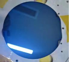
Coating Samples
Process Steps
→ Place the substrate for coating into the vacuum chamber;
→ Vacuumize the vacuum chamber at high and low temperature, and rotate the substrate synchronously;
→ Start coating: the substrate is contacted with precursor in sequence and without simultaneous reaction;
→ Purge it with high-purity nitrogen gas after each reaction;
→ Stop rotating the substrate after the film thickness is up to standard and the operation of purging and cooling is
completed, then take out the substrate after the vacuum breaking conditions are met.
Our Advantages
We are manufacturer.
Mature process.
Reply within 24 working hours.
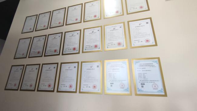
Our ISO Certification
Parts Of Our Patents 
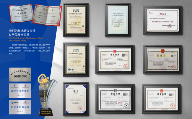
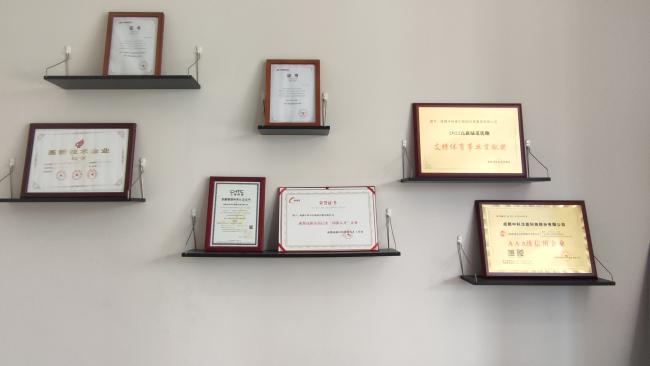
Parts Of Our Awards and Qualifications of R&D
Get in Touch
Have questions about our products or want to discuss a custom order? Our team is ready to help you.