
Micro Electro Mechanical Systems MEMS Atomic Layer Deposition Equipment Lubricating Coating
Atomic Layer Deposition in Micro Electro Mechanical Systems Industry
Applications
| Applications | Specific Purpose |
|
Micro Electro Mechanical Systems (MEMS) |
Anti-wear coating |
| Anti-adhesion coating | |
| Lubricating coating |
Working Principle
A single atomic layer will be deposited in each process cycle. The coating process usually occurs in the reaction
chamber, and the process gases are injected successively. Alternatively, substrate can be transferred between two
zones filled with different precursors (spatial ALD) to realize the process. The entire process,including all reactions
and purging operations, will be repeated again and again until the desired film thickness is realized. The specific
initial phase state is determined by the surface properties of the substrate, and then the film thickness will rise
constantly with the increase of the reaction cycle numbers.So far, the film thickness can be controlled accurately.
Features
| Model | ALD-MEMS-X—X |
| Coating film system | AL2O3, TiO2, ZnO, etc |
| Coating temperature range | Normal temperature to 500℃ (Customizable) |
| Coating vacuum chamber size |
Inner diameter: 1200mm, Height: 500mm (Customizable) |
| Vacuum chamber structure | According to customer’s requirements |
| Background vacuum | <5×10⁻⁷mbar |
| Coating thickness | ≥0.15nm |
| Thickness control precision | ±0.1nm |
| Coating size | 200×200mm² / 400×400mm² / 1200×1200 mm², etc |
| Film thickness uniformity | ≤±0.5% |
| Precursor and carrier gas |
Trimethylaluminum, titanium tetrachloride, diethyl zinc, pure water, |
| Note: Customized production available. | |
Coating Samples


Process Steps
→ Place the substrate for coating into the vacuum chamber;
→ Vacuumize the vacuum chamber at high and low temperature, and rotate the substrate synchronously;
→ Start coating: the substrate is contacted with precursor in sequence and without simultaneous reaction;
→ Purge it with high-purity nitrogen gas after each reaction;
→ Stop rotating the substrate after the film thickness is up to standard and the operation of purging and cooling is
completed, then take out the substrate after the vacuum breaking conditions are met.
Our Advantages
We are manufacturer.
Mature process.
Reply within 24 working hours.
Our ISO Certification

Parts Of Our Patents


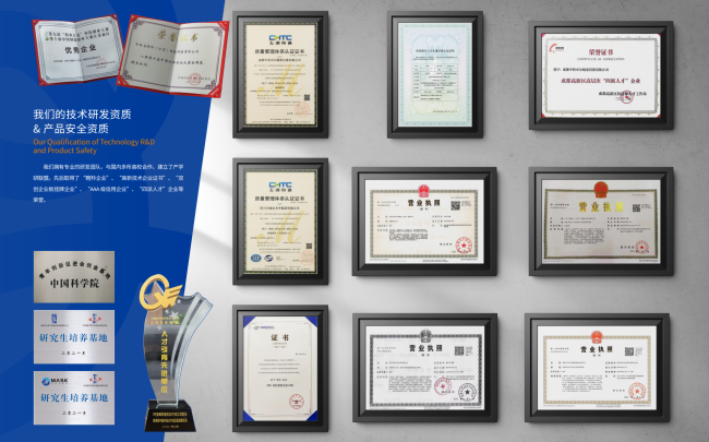
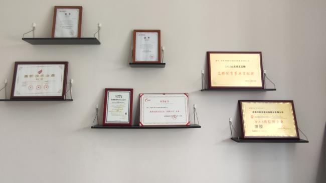
Parts Of Our Awards and Qualifications of R&D
Get in Touch
Have questions about our products or want to discuss a custom order? Our team is ready to help you.