
Red Solder Mask 4 Layer PCB 1.6 MM Thickness 1 OZ Copper
4 Layer PCB 1.6 MM Thickness 1 OZ Copper Red Solder Mask
- Main Features:
1 4 Layer Printed Circuit Board PCB .
2 Immersion Gold treatment, gold thickness 1u'.
3 FR4 substrate material, tg150 degree.
4 Min line space and width 6/6mil.
5 Copper thickness is 1 oz on each layer, 35 um on each layer.
6 Black solder mask and white silkscreen.
7 ROHS, MSDS, SGS, UL, ISO9001&ISO14001 Certificated
- Our Product Categories:
| Our Product Categories | ||
| Material Kinds | Layer Counts | Treatments |
| FR4 | Single Layer | HASL Lead Free |
| CEM-1 | 2 Layer/Double Layer | OSP |
| CEM-3 | 4 Layer | Immersion Gold/ENIG |
| Aluminum Substrate | 6 Layer | Hard Gold Plating |
| Iron Substrate | 8 Layer | Immersion Silver |
| PTFE | 10 Layer | Immersion Tin |
| PI Polymide | 12 Layer | Gold fingers |
| AL2O3 Ceramic Substrate | 14 Layer | Heavy copper up to 8OZ |
| Rogers, Isola high frequency materials | 16 Layer | Half plating holes |
| Halogen free | 18 Layer | HDI Laser drilling |
| Copper based | 20 Layer | Selective immersion gold |
| 22 Layer | immersion gold +OSP | |
| 24 Layer | Resin filled in vias | |
- FAQ:
Q1: What is PCB Bow and Twist?
A1: PCB Bow and Twist are parameters that determine alignment errors in a PCB board based on its flatness. The PCB Bow tests the spherical or cylindrical curvature of the board, when its four corners lie in the same plane. The PCB twist tests if any one corner of the PCB is different from the others four in terms of flatness. A board with a bow issue will lift off the surface despite all corners of the board making contact with the plane. The twist occurs when three of the PCB corners are in contact with the surface while the fourth corner is elevated.
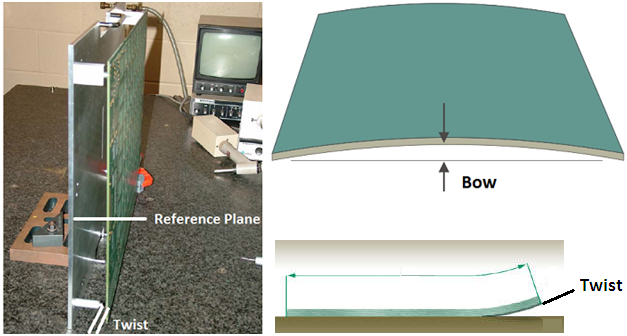
According to the IPC-A-600 standard, boards with less than 1.5% of bow and twist are acceptable. In the case of the boards with SMD components, this percentage needs to be less than 0.75%.
PCB Bow and Twist can be used by a number of factors that include high temperature exposure, heavy thermal shocks during soldering etc. The board design, thickness, layers and materials also play a role in the board showing Bows and Twists over various fabrication, assembly or operating conditions.
Get in Touch
Have questions about our products or want to discuss a custom order? Our team is ready to help you.