
Red Solder Mask FR4 Circuit Board 1 OZ Copper Thickness OSP Treatment
Red Solder Mask FR4 Substrate Material 1 OZ Copper Thickness OSP Treatment
PCB Specifications:
1 Part NO: Multi-Layer PCB000351
2 Layer Count: 8 Layer PCB
3 Finished Board Thickness: 1.6MM
4 Copper Thickness: 1/1/1/1/1/1 OZ
5 Min Lind Space&Width: 3.5/3.5 mil
6 Application Area: Amplifier
Material Data Sheet:
| S1000-2 | |||||
| Items | Method | Condition | Unit | Typical Value | |
| Tg | IPC-TM-650 2.4.25 | DSC | ℃ | 180 | |
| IPC-TM-650 2.4.24.4 | DMA | ℃ | 185 | ||
| Td | IPC-TM-650 2.4.24.6 | 5% wt. loss | ℃ | 345 | |
| CTE (Z-axis) | IPC-TM-650 2.4.24 | Before Tg | ppm/℃ | 45 | |
| After Tg | ppm/℃ | 220 | |||
| 50-260℃ | % | 2.8 | |||
| T260 | IPC-TM-650 2.4.24.1 | TMA | min | 60 | |
| T288 | IPC-TM-650 2.4.24.1 | TMA | min | 20 | |
| T300 | IPC-TM-650 2.4.24.1 | TMA | min | 5 | |
| Thermal Stress | IPC-TM-650 2.4.13.1 | 288℃, solder dip | -- | 100S No Delamination | |
| Volume Resistivity | IPC-TM-650 2.5.17.1 | After moisture resistance | MΩ.cm | 2.2 x 10⁸ | |
| E-24/125 | MΩ.cm | 4.5 x 10⁶ | |||
| Surface Resistivity | IPC-TM-650 2.5.17.1 | After moisture resistance | MΩ | 7.9 x 10⁷ | |
| E-24/125 | MΩ | 1.7 x 10⁶ | |||
| Arc Resistance | IPC-TM-650 2.5.1 | D-48/50+D-4/23 | s | 100 | |
| Dielectric Breakdown | IPC-TM-650 2.5.6 | D-48/50+D-4/23 | kV | 63 | |
| Dissipation Constant (Dk) | IPC-TM-650 2.5.5.9 | 1MHz | -- | 4.8 | |
| IEC 61189-2-721 | 10GHz | -- | — | ||
| Dissipation Factor (Df) | IPC-TM-650 2.5.5.9 | 1MHz | -- | 0.013 | |
| IEC 61189-2-721 | 10GHz | -- | — | ||
| Peel Strength (1Oz HTE copper foil) | IPC-TM-650 2.4.8 | A | N/mm | — | |
| After thermal Stress 288℃,10s | N/mm | 1.38 | |||
| 125℃ | N/mm | 1.07 | |||
| Flexural Strength | LW | IPC-TM-650 2.4.4 | A | MPa | 562 |
| CW | IPC-TM-650 2.4.4 | A | MPa | 518 | |
| Water Absorption | IPC-TM-650 2.6.2.1 | E-1/105+D-24/23 | % | 0.1 | |
| CTI | IEC60112 | A | Rating | PLC 3 | |
| Flammability | UL94 | C-48/23/50 | Rating | V-0 | |
| E-24/125 | Rating | V-0 | |||
FAQ:
Q1: What are PCB Mouse bites?
A1:
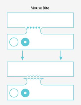
Mouse bites also known as perforated breakaway tabs in a PCB are small perforations / pricks on the board which allow for panelizing and depanelizing smaller groups of PCBs together. This way multiple PCB boards can be assembled together, thereby saving time and making the process cost-effective. The assembled PCBs can be separated by applying pressure on the sections of the board that have perforations. Once separated, i.e after the depanelization process, the board looks like it has mouse bites in these sections.
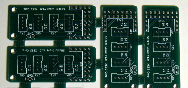
Below is an Image of PCBs assembled to each other with the help of mouse bites.
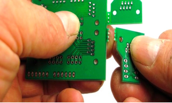
Below is an Image of a PCB being depaneled easily which is also made possible due to mouse bites. You can also see the sharp edges after the boards have been separated, these are called mouse bites.
When multiple PCBs are connected using mouse bites they have a smooth finish. When compared to PCB boards connected using V-Scoring, boards connected with mouse bites are easier to depanelize i.e they require less force.
Precautions to take before inserting Mouse bites on a PCB
- Develop an adequate number of mouse bites to support a board completely when paneled with other boards
- Do not place the mouse bites close to sensitive component areas or circuitry. This will cause the board to experience breakout stress which can damage sensitive components or sections of the board
- The spacing between two mouse bites must range between 60mm to 90mm
Get in Touch
Have questions about our products or want to discuss a custom order? Our team is ready to help you.